PCB Design with KiCad
Example Project
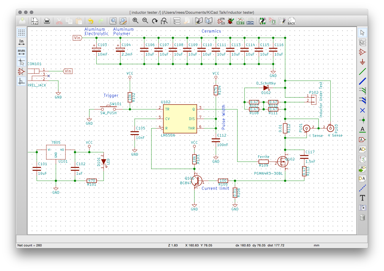
A tool for measuring inductors. Inductors are important especially in circuits involving higher currents, but they can be hard to measure.
\[ V = L \frac{dI}{dt} \]Or, in English, the voltage across the inductor is equal to it's inductance times the change in current through the inductor. This circuit will apply a constant voltage step, and allow us to measure \(dI/dt\) so we can find \(L\).
Design Notes
- Good discussion of similar tools including example output here, or here.
- Three types of capacitor to get large C & low ESR/ESL.
- Added voltage output so can correct for change in voltage step (and show when tester runs out of steam).
- Pads for snubber and gate drive resistor/bead just in case.
- Diode + resistors to dump energy from inductor.
- Fixed pulse width.(oversight: if the trigger is held down, will get longer pulse...)
- Current sense polarity is intentionally reversed.
- Mounting: Hot glue and PLA!
Basic PCB Terminology
- Solder Mask - The green stuff.
- Track - Copper "wire" on the PCB.
- Net - Logical connection between points in a schematic.
- Via - Connection between tracks on different layers.
- Footprint - Provision for attaching a part to a PCB.
- BOM - Bill Of Materials (list of parts).
Workflow
"KiCad" is a collection of several programs, each with their own role in the PCB design process.
- KiCad - Organises projects / launches other programs
- Eeschema - Schematic capture
- Pcbnew - PCB Layout
- GerbView - Gerber file viewer
KiCad
KiCad is designed around working on one project at a time, each PCB project is kept in it's own directory.
Eeschema
What is "schematic capture"? It's all about drawing the schematic (aka circuit diagram), which produces the netlist and BOM. The netlist is required for PCB layout, or can be used for running simulations in SPICE. More below.
UI involves using keyboard + mouse, you'll want to learn some of the keyboard shortcuts.
- ESC - normal cursor
- Return - repeat last
- a - Add component (defaults to last used)
- m - Move object (breaks connections)
- g - Grab object (moves connections, tab for groups?)
- p - Power node
- v - Value of the part
- w - Wire
Wires can be connected to other wires (filled green circles) or unconnected pins (square/circle outlines).
General workflow is to move cursor to start of wire, press 'w' key, draw wire, pressing 'w' to add corners, then click a node or press 'k' to end the wire.
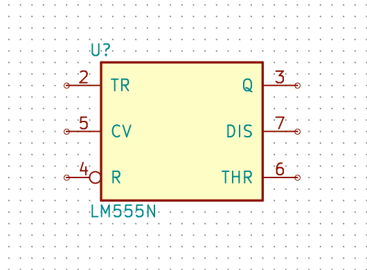
Where are pins 1 and 8? Some parts have pins that are hidden by default - see the "Show hidden pins" button on the left. Make sure a net has name "VCC" to provide power to these.
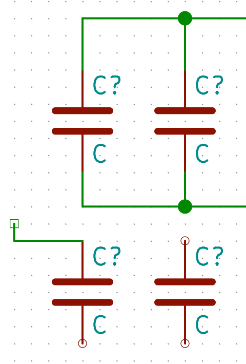
Once the diagram has all required parts, "Annotate" it to change reference designators from C? to C123.
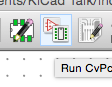
Next, we need to associate the parts on the schematic with footprints for the PCB Layout tool. Run the CvPcb tool with the button at the top:
CvPcb shows three panes - the left pane is a list of parts libraries, the middle is the parts in your schematic, and the right is a list of parts that have passed through the current set of filters. Filters are enabled/disabled using the buttons at the top. Associate parts by highlighting your part in the middle, then double clicking the footprint on the right.
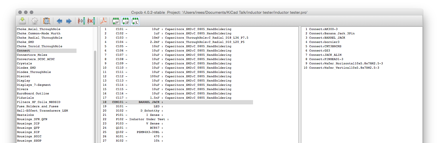
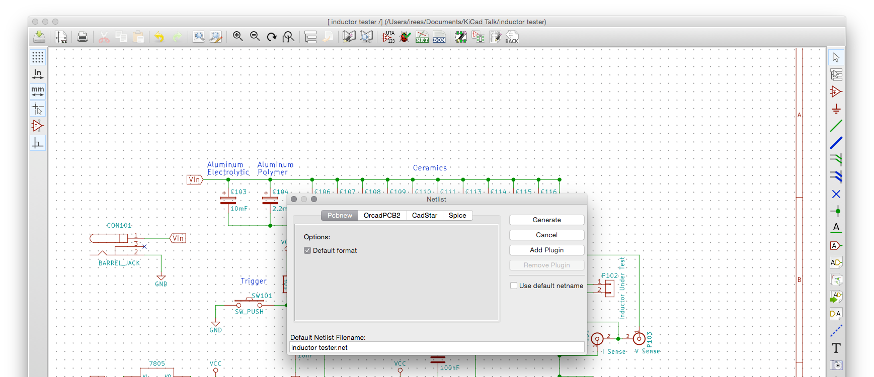
Once all the parts on your board are associated with footprints, click the "save" button and go back to Eeschema to export the netlist. Default settings should be fine for Pcbnew.
Pcbnew - PCB Layout
Pcbnew is the program where we do the actual circuit board layout. It takes a netlist from Eeschema and footprint information from the library, and helps you lay out a PCB.
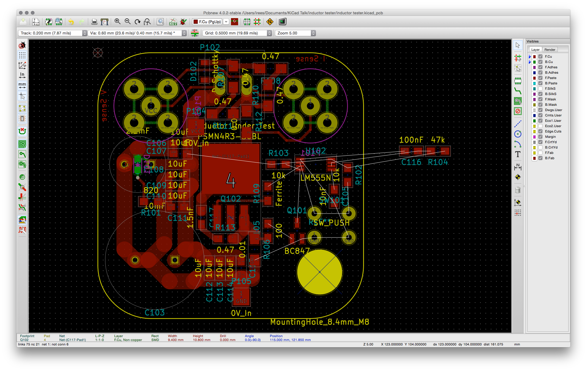
What am I looking at?
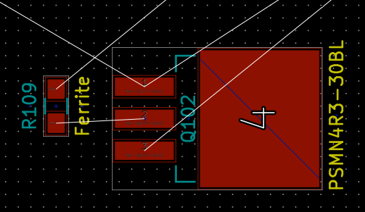
- Thin white lines are the "Rat's nest". These are connections that need to be made.
- Different colours mostly represent different layers in the "stack up", but a few are intended to help with design or assembly. See the bar on the right.
- "Edge.Cuts" is the border of the PCB.
Units
PCBs dimensions are often discussed in mils, which is prounounced "terrible unit". A mil is \(\frac{1 inch}{1000}\), not a millimeter.
Things get especially fun with SMT package sizing eg 0603 Metric is equivalent to 0201 Imperial, about a third the size of the more common 0603 Imperial.
You'll find some parts fit nicely on mm grids, and some fit nicely on inch grids. So, don't get too caught up on one system or another - it's very easy to switch the grid as desired.
The first step using Pcbnew in a new project is importing the netlist from your earlier work in Eeschema. Click the "Read netlist" button to bring in your earlier work - it should be selected by default. You might get a few errors like these - we'll deal with them later:
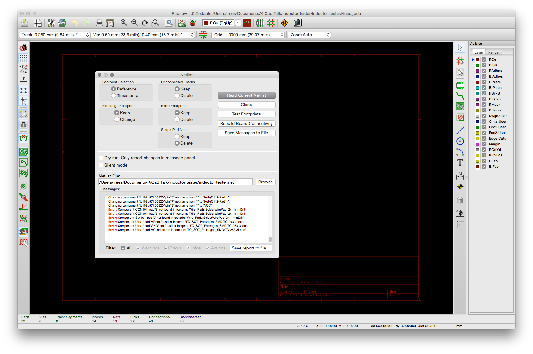
Once your netlist is imported, all the parts will be stacked on top of each other - not very helpful.
Make sure you're in "Footprint mode" 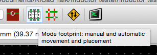 , then right click in the black area and select "Global Spread and Place", then "Spread out All Footprints".
In my experience, PCB layout is an iterative process. This time, we know the maximum dimensions based on the PCB supplier - it's cheaper if we can stay inside 5x5 cm - so let's start making a board outline. Pick the Edge.Cuts layer on the right hand side, then select the "Add Graphic Line or Polygon".
While getting the outline right, you might find it helpful to right-click on sections of the "drawing" (the outline) with the drawing tool selected. For example, the arc tool will create 90° arcs by default, but those can be changed through the "Edit Drawing" context menu.
Unfortunately, there's an error in the netlist generated - the gate pin on this FET should be pin 1, but we've got it connected to pin 2... How to fix
Some of the track in this project will need to carry relatively high current, so we'll want to draw those a bit wider than default. Pcbnew uses a concept of "Net Classes" to set default widths, clearances, via sizes, etc. for nets. Net Classes are setup in Design Rules > Design Rules Editor.
For a simple board, make sure the clearance for the default net list looks reasonable, then go to the Global Design Rules tab and add some extra track width and via diameters.
The "add tracks and vias" tool lets you lay down wires. When you're drawing, the 'w' key changes width, and the 'v' key adds a via.
Symbols & Footprints
Although KiCad has a large libary of components available, we'll likely need to make some additions or changes. In doing this, it's important to understand the distinction between a Symbol and Footprint (formerly known as module).
- Symbol - Stored in a Library, is the thing that you see on the schematic/circuit diagram. Make changes/additions to symbols via Eeschema.
- Footprint - Stored in a .pretty directory, represents the physical device on the PCB, modified in Pcbnew.
I've found three approaches to footprint issues in KiCad:
- Make an entirely new Symbol and Footprint
- Modify an existing Symbol/Footprint
- Make a one-off modification to the Footprint in Pcbnew
Modifying Symbols
There's probably a better way to do this...- Back in Eeschema, find the offending symbol.
- Right click, "Edit Component > Edit Component in Library Editor".
- Fix the part - in this case, change pin assignments by putting the cursor over the pin to change and pressing "e".
- Save the current component to a new library. Put the new library in the project folder if you intend to share it.
- Close the Part Library Editor.
- Back in Eeschema, "Preferences > Component Libraries".
- Click the top "Add" button and navigate your new library.
- Right click the symbol again, click "Edit", then click "Select" in the "Chip Name" box.
- Press OK in the Edit dialog. It may be hidden behind Eeschema (Mac only?).
One-off footprint changes
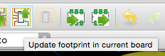
- In Pcbnew, right click the [placed] footprint, then "Edit with Footprint Editor".
- Make changes to the footprint as desired (hold cursor over pad and press 'e' to change pin numbers)
- Click the "Update footprint in current board" button.
Exporting
PCB fab houses generally take "Gerbers" for everything except the "drill file", which uses Excellon format. Generate Gerbers from Pcbnew's file > Plot dialog.
Dirty PCBs
I've had good experiences ordering boards from Dirty PCBs and would recommend them, especially for hobby usage. They requires gerber files to be submitted in a particular format; see their about page for details. In Pcbnew's Plot dialog, tick the "Use Protel filename extensions" box to get 90% of the right format, AFAIK only the Edge.Cuts will need to be renamed.
General Notes
- File formats used in KiCad are "plain text", so work nicely with revision control systems.
- Presentation made with reveal.js
- KiCad homepage
- Plenty resources on the net - eg this YouTube video or forums, but keep in mind that KiCad is improving quickly and there is outdated information around.